



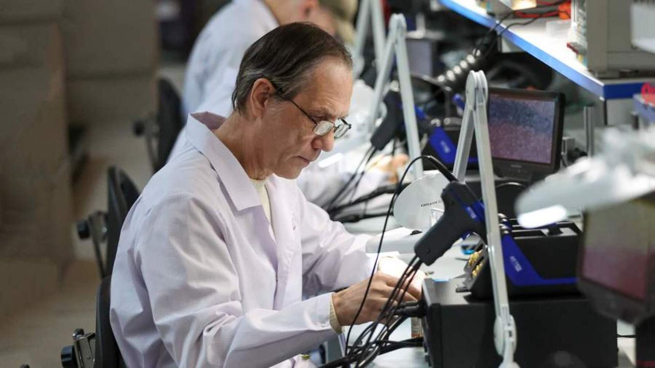
- Russian multicathode built and tested, but full lithography machine still years away from existing
- Wafer exposure could drop from two weeks to five minutes flat
- Electron beam tips measure just 1.5 to 2 nanometers wide
A Russian startup has unveiled a multipath electronic lithograph project intended to manufacture modern microchips at significantly greater speed than before.
The core technology is a multicathode capable of generating multiple electron beams simultaneously, which has reportedly been built and tested by engineers.
Developers say the device could expose a silicon wafer in roughly five to seven minutes, compared with one to two weeks for older single-beam machines.
Multicathode breakthrough
“We have developed an end-to-end technology for creating a multicathode and confirmed its operability in practice,” said Evgeny Givargizov, the project’s main developer.
He added that arrays of these electron sources rank among the sharpest ever produced, with tip radii of only 1.5 to 2 nanometers.
Unlike many foreign multipath systems that rely on complex beam-splitting optics with mirrors and shutters, the Russian design creates independent sources directly on one substrate.
This approach could lower engineering complexity, reduce energy consumption, and cut equipment costs relative to conventional single-beam lithography systems.
The project was first unveiled publicly at the Strong Ideas for Modern Times forum, where researchers described the completed research phase.
The developed and tested multicathode is only the electron-beam source, one component of the planned lithography machine.
Officials clarified that no finished lithography machine exists yet, since only the scientific research stage has so far concluded successfully.
The upcoming development phase is expected to focus mainly on building the full lithograph around the already validated multicathode source.
Long road to industrial use
Sergey Sazonov, a microelectronics expert at Russia’s National Technology Initiative, described the concept as promising if multicathode control proves reliable at scale.
“The technology looks interesting and promising, but there is still a lot of work to be done before an industrial alternative emerges,” said Sazonov.
Engineering specialist Sergey Varnavsky offered a more cautious view, noting that only the multicathode component currently exists in working form.
He warned that prolonged funding delays could allow rival technologies abroad to advance further before any finished lithograph reaches production.
Even so, he suggested limited competition within Russia’s domestic market could still create demand among local chip and circuit board manufacturers.
Varnavsky noted that overall success would depend heavily on securing consistent funding through every remaining stage of the project’s testing.
Developers estimate a working prototype could take roughly three years to build, spanning chip standards from 350 nm down to a few nanometers.
According to the team, maximum resolution today depends mainly on available photoresist materials rather than the electron beam source itself.
This distinction suggests that future resolution improvements may still hinge on materials science advances rather than further electron optics breakthroughs.
For now, the multicathode remains a promising laboratory result rather than proof that Russia can rival established chipmaking equipment leaders like IMEC.
Via Izvestia (originally in Russian)